🌈 ESP32-S3 Rainbow: ZX Spectrum Emulator Board! Get it on Crowd Supply →
View All Posts
read
Want to keep up to date with the latest posts and videos? Subscribe to the newsletter
HELP SUPPORT MY WORK: If you're feeling flush then please stop by Patreon Or you can make a one off donation via ko-fi

Is SOT666 Really Standard? Spoiler: Not Really

I’ve been investigating some quality assurance failures on my ESP32 rainbow boards and tracked a few issues down to a USBLC6 ESD protection IC in a SOT666 package. Under the microscope, it looked like the footprint didn’t quite match the package — like it had missed alignment and hadn’t soldered on properly.

I fixed the immediate problem by reflowing the solder and pushing the device into place. But this should be automatic — the pick and place machine puts the component down and solder tension should pull it into alignment. So I started wondering: is the footprint actually correct?

The Problem: Footprint vs Datasheet

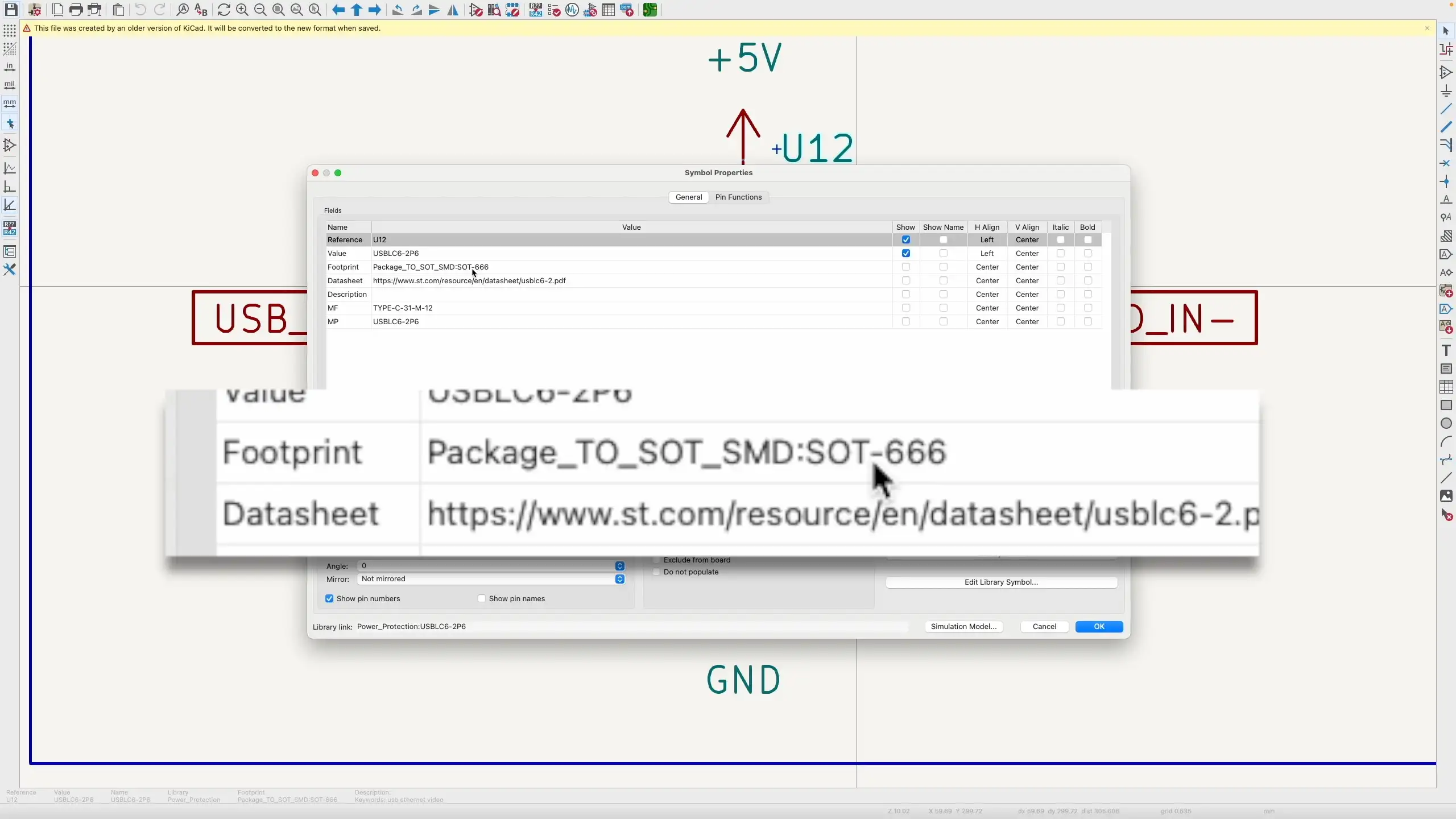
Opening up the schematic in KiCad, the USBLC6 is assigned a SOT666 footprint. That’s the correct package — so far so good.

KiCad schematic showing the USBLC6 with SOT666 footprint

But when I compared the KiCad footprint against the recommended footprint in the USBLC6 datasheet, things looked pretty different.

KiCad footprint vs datasheet recommended footprint

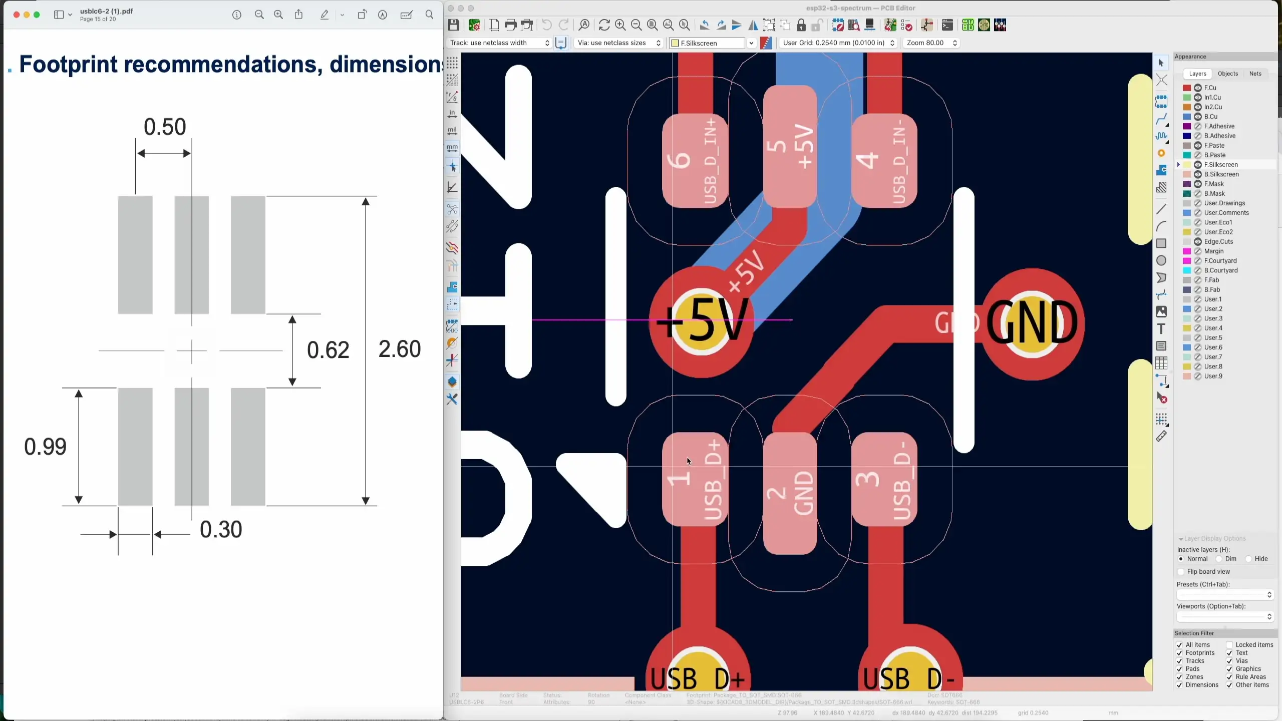
The KiCad footprint for SOT666 is completely different from the footprint in the datasheet — even though they’re both supposed to be SOT666.

So Is KiCad Wrong?

Maybe. But it’s not that simple.

If you Google “SOT666” you’ll find all sorts of different footprints from different manufacturers. Here’s how they stack up:

  • Nexperia’s SOT666 definition — looks very similar to KiCad’s version. In fact, I think KiCad’s footprint is based on this one.
  • ST’s USBLC6 datasheet — has its own recommended footprint with quite different dimensions.
  • Diodes Incorporated’s SOT666 — yet another completely different suggested pad layout.

Different SOT666 footprints from different manufacturers

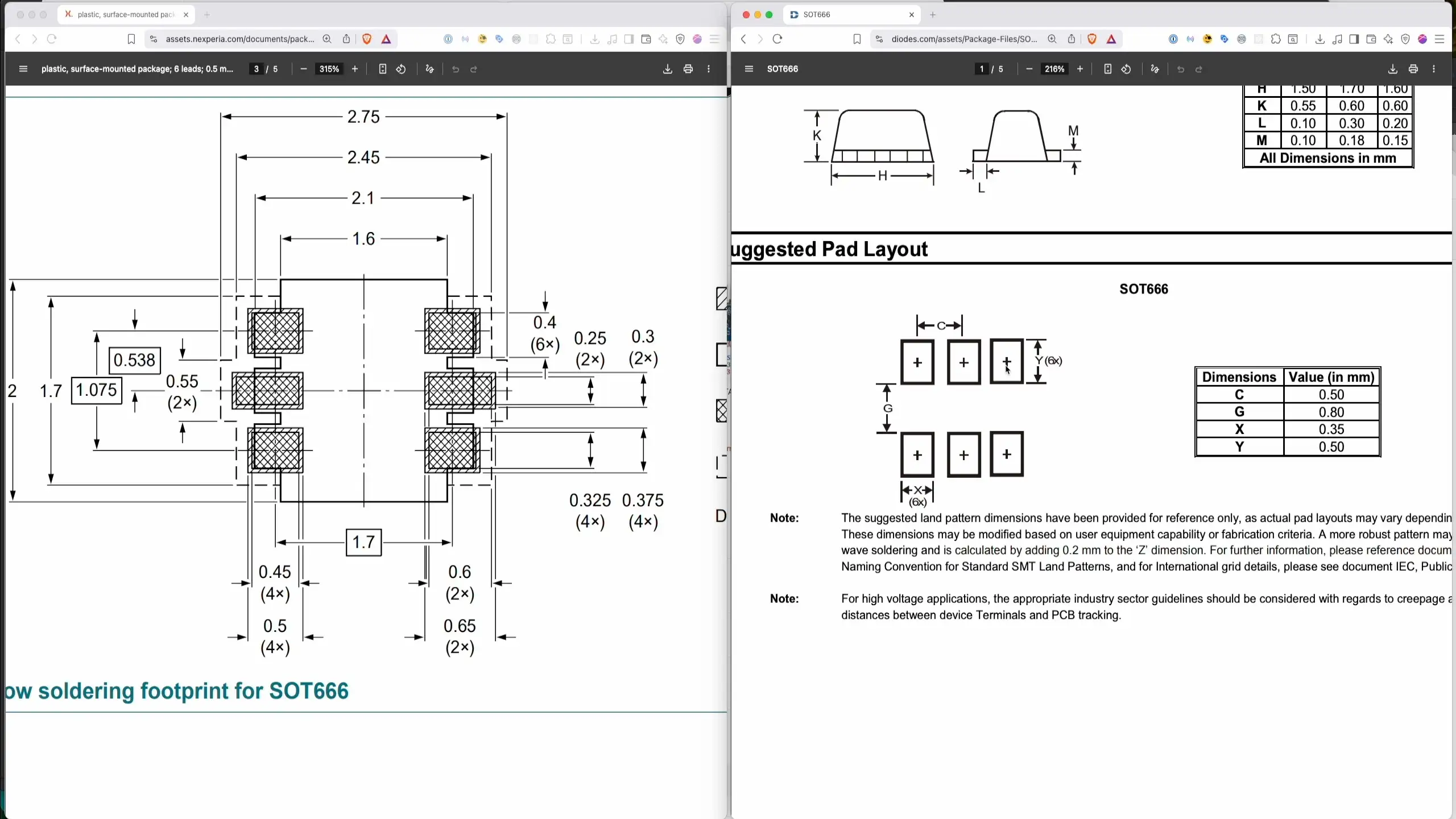
So you’ve got a “standard” package name — SOT666 — but every manufacturer seems to have their own opinion about what the footprint should look like.

Checking EasyEDA for Comparison

I thought it might be instructive to check another EDA package. In EasyEDA, the SOT666 footprint for the USBLC6-2P6 is different again:

  • Pad width (PW1): 0.3 mm — this actually matches the ST datasheet
  • Pad length (PL1): 0.85 mm — the ST datasheet says 0.99 mm, so still different

What does EasyEDA think?

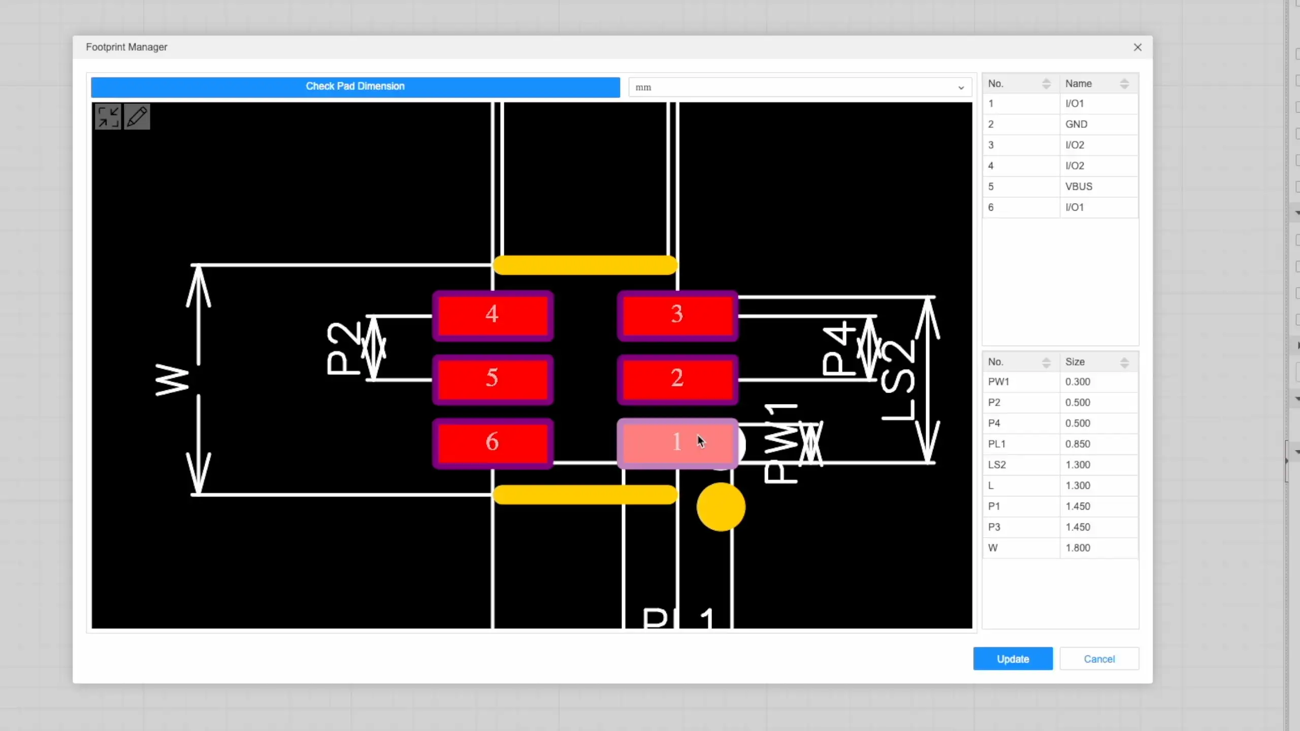
Three different tools, three different footprints, all for the same “standard” package. Not exactly confidence-inspiring.

The Lesson: Always Follow the Datasheet

The basic conclusion is that although these packages share the same name, the footprints are not really standardised. Everything is randomly different.

The advice: look in the datasheet and use what’s in the datasheet. Don’t rely on the standard package names because they might not quite match up with your specific component.

Creating a Custom Footprint in KiCad

Fortunately, it’s really easy to create footprints in KiCad. Using the footprint wizard with the SOIC template, I just needed to plug in the values from the ST datasheet:

  • Pad count: 6 (two rows of 3)
  • Pitch: 0.5 mm
  • Pad width: 0.3 mm
  • Pad length: 0.99 mm
  • Row spacing: 1.61 mm (0.62 mm gap + 0.99 mm pad length)

KiCad footprint wizard with datasheet values

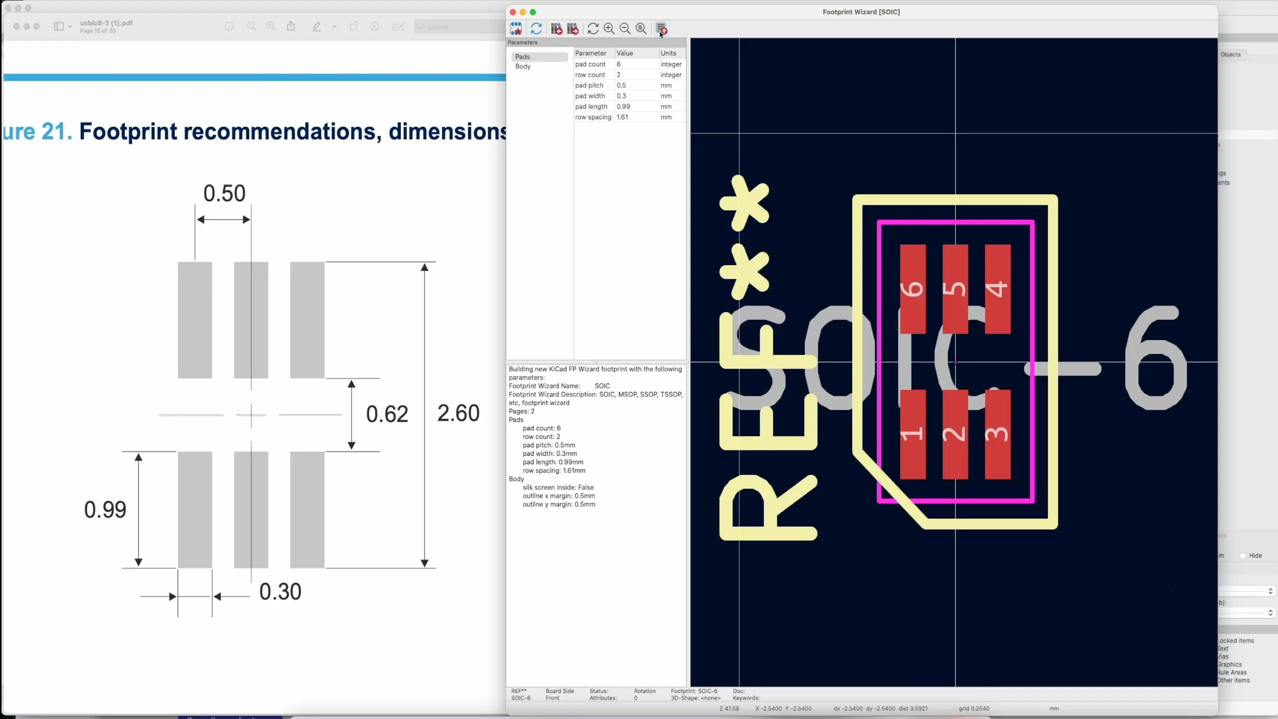
A quick sanity check with the ruler confirmed everything matched the datasheet — the 0.62 mm gap between rows and 2.6 mm overall dimensions were spot on.

Updating the PCB

It took a bit of finagling — I had to make some traces slightly thinner so they didn’t collide — but the new footprint dropped into the design nicely.

Updated PCB with the new footprint

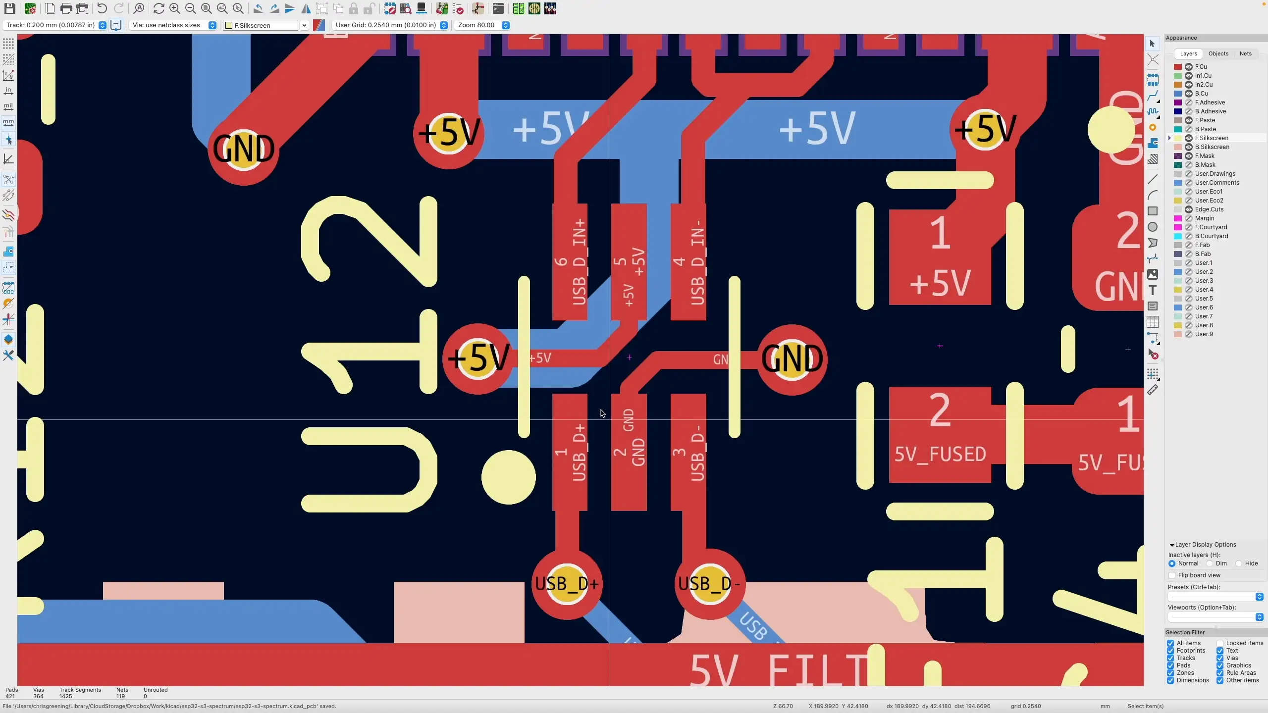
The 3D preview looks good. Obviously the proof of the pudding will be the next production run, but it matches the datasheet now — so fingers crossed it will eliminate this class of QA errors.

Wrapping Up

If you’re designing PCBs, don’t assume that a standard package name means a standard footprint. Always cross-reference with your specific component’s datasheet. It only takes a few minutes to create a custom footprint in KiCad, and it could save you from chasing down mysterious assembly failures.

Related Posts

ESP32 Rainbow QA - A tale of three boards - We’ve shipped a few hundred ESP32 Rainbow boards-most are perfect - but a few failed QA. Here’s how we tracked down and fixed three real-world faults: no sound from lifted headphone jack pads, USB not enumerating due to a mis-seated ESD IC pin, and a flaky touch keyboard from poor ESP32 module joints. A bit of microscope work and reflow brought two boards back to life (one’s now a donor), and it’s a great reminder why we do final assembly and full QA here in Scotland.
A Potentially Explosive Error - Just received the new PCBs for the ESP32-TV project and they're looking sharp with only a tiny resistor tweak needed. But I discovered a sneaky, undocumented resistor causing a conflict between the ESP32 and USB2244 over the USB connection. Fixed that, but there's a bigger issue lurking in the design - check the schematic in the video and see if you can spot it before I reveal the explosive mistake!
When “Software Bugs” Are Actually Bad Soldering - A quick MLX90640 IR camera test turned into a dead-on-I2C mystery. I ran the usual checks—addresses, pull-ups, voltages, wiring—and even fixed my forgotten UART/I2C jumper, but still nothing. A peek under the microscope revealed sketchy solder on the 3V3 LDO; a quick reflow and the sensor sprang to life. Lesson relearned: don’t trust factory soldering, look early with a microscope, and stop blaming software when the hardware’s silent.
ESP32-S3 Dev Board Assembly - I finally assembled our ESP32-S3 dev boards—used a stencil for easy SMD work, fixed a few tiny USB solder bridges with flux, and even hand-built one for fun. The EPAD isn’t required (per the datasheet), power LEDs look good, and on macOS you can spot it under /dev before flashing. A quick boot-button dance and the blink sketch runs great—full build and walkthrough in the video.
I broke it and then i fixed it - Started off on a techie adventure with an RP2040 DVI board from Adafruit, aiming to get the pico-zxspectrum going. Things started acting haywire once the USB hub got involved, ending in a complete shutdown, intuitive diagnosis showed the power pin was a ghost town! After pin-pointing (and removing) the dead IC, I performed a delicate soldering operation to bless it with a new 3V3 regulator. Working the kinks out with the resolution led to a thrilling revival and, voila, we were back in business with DVI output and SD Card support!

Related Videos

I Thought SOT666 Was a Standard - It Isn’t. - I tracked some QA failures on my ESP32 rainbow boards down to the USBLC6 ESD IC in a SOT666 package—under the microscope the part wasn’t actually landing on the pads. Reflowing fixed it, but that shouldn’t be necessary, so I compared KiCad’s SOT666 footprint to the ST datasheet and found big mismatches. Turns out “SOT666” isn’t consistent across vendors (KiCad/Nexperia/Diodes/EasyEDA all differ), so the only safe move is to follow the exact datasheet for the specific part. I built a new footprint in KiCad per ST’s land pattern, tweaked the routing, and the 3D preview looks good—fingers crossed the next run nails it.
Three ESP32 Rainbow Boards Failed QA — Can we fix them? - I’m assembling another batch of ESP32 Rainbows: PCB house does the boards, UV silkscreen and some parts, and I finish assembly and QA here in Scotland. I run through three QA fails—no sound, dodgy keyboard, and no USB—then fix two: the audio fault was lifted pads on the headphone jack, so I bodged it back with flux and solder (speaker and headphones now work, but it’s a spares board). The no‑USB issue was an ESD protection IC sitting off its pad; I reflowed it on a mini hot plate, cleaned up with IPA, verified continuity, and it now enumerates and flashes perfectly. On to the keyboard next—oh, and Happy New Year!
Super Easy ESP32-S3 Dev Board - Making an ESP32-S3 dev board is way easier than it looks. I simplify the datasheet reference: skip the external crystal, wire native USB D+/D− (pins 19/20) straight to a USB-C with 5.1k CC pulldowns, add a BOOT switch and an EN RC reset, and power it with an LD117 LDO that’s happy with ceramic caps. In KiCad I build the schematic with Espressif libraries, add LEDs for 5V, 3V3, and a blink GPIO, set up net classes, route a clean USB differential pair, stitch a solid ground plane, and label everything. It’s a bit wide—just gang breadboards together—and you end up with a neat, professional S3 dev board you can flash and debug over USB.
World’s Smallest USB-C Li-Ion Charger?! - I found some super compact USB-C lithium battery chargers on AliExpress, and they're tiny! The PCB is just 10mm by 6mm, but it packs a punch with a linear lithium-ion battery charger chip, LP 4054. It's equipped with indicator LEDs for charging status and includes essential resistors and capacitors. Be cautious, though, as it can get warm during use. I've decided to recreate this neat design in Keycad, showing you each step, paying tribute to our Patreons and PCB Way along the way. Let's see how the design translates and if it passes all checks!
How Good Are My USB Cables? - In this video, I engage in a deeper exploration of USB testing, encountering a range of trials and tribulations along the way. First up, I attempt to test a couple of USB cables and discuss their data lines' peculiar situatedness. Then, I delve into the assembly of the PCB boards, sourced from PCBWay, which surely turned into a learning voyage than an easy sail. The first version faced challenges of misordered large-frame stencil, unseen connection problems, and even DRC errors in the submission process. Not dwell on that, I redesign and bring to table Version 2, complete with USB connectors with broken-out pins and designed for visual inspection ease. Although this version demonstrated success, soldering difficulties and bad connections persisted. Considering all the hurdles, I decide to let PCBWay handle the assembly for the next version. For future strategies, adding test points and eliminating the lithium-ion charging circuit seemed more practically viable. Peeping into version 3, testing points for all USB cable pins have been added and even an option to break out actual USB connections, all towards ensuring an improved error checking and usefulness of the assembly.
HELP SUPPORT MY WORK: If you're feeling flush then please stop by Patreon Or you can make a one off donation via ko-fi
Want to keep up to date with the latest posts and videos? Subscribe to the newsletter
Blog Logo

Chris Greening


Published

> Image

atomic14

A collection of slightly mad projects, instructive/educational videos, and generally interesting stuff. Building projects around the Arduino and ESP32 platforms - we'll be exploring AI, Computer Vision, Audio, 3D Printing - it may get a bit eclectic...

View All Posts